
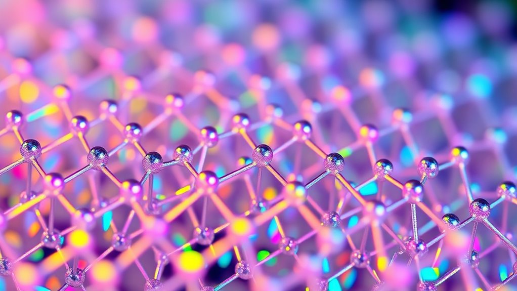
Photonic crystals are structures designed at the nanoscale to manipulate light by creating periodic variations in refractive index. These arrangements produce photonic band gaps that prevent certain wavelengths from propagating, allowing precise control over light flow. Different forms, from 1D to 3D, offer unique ways to confine and guide light efficiently. As you explore further, you’ll discover how advances in fabrication and applications are shaping the future of optical technology.
Key Takeaways
- Nanoscale chemistry enables precise fabrication of photonic crystal structures with controlled refractive index contrasts.
- Chemical methods facilitate the self-assembly of nanostructures that form periodic patterns for light manipulation.
- Material chemistry influences the bandgap tuning, allowing customization of photonic properties for specific wavelengths.
- Surface functionalization and chemical treatments improve defect control and structural stability in photonic crystals.
- Advances in nanoscale chemistry support integration of photonic crystals with electronic devices for enhanced optical performance.
What Are Photonic Crystals and How Do They Work?
Have you ever wondered how engineers control light with such precision? Photonic crystals are advanced nanostructures that do just that. They’ve a repeating pattern in their refractive index, which blocks certain light wavelengths—creating a photonic band gap, much like an electronic band gap in semiconductors. Color fidelity is also influenced by these structures, as their ability to manipulate specific wavelengths can enhance or diminish color accuracy in optical devices. These structures can be one-, two-, or three-dimensional, influencing light in different ways. When designed properly, they guide, reflect, or confine specific wavelengths. By adjusting their size, shape, and periodicity, you can tailor the band gap to target particular colors of light. Material properties with alternating refractive indices form the core of these crystals, enabling precise control over light flow at the nanoscale. Understanding the band gap phenomenon is crucial for developing advanced optical devices and integrated photonic circuits. This control is essential for developing advanced optical devices and integrated photonic circuits.
The Significance of Nanoscale Periodicity in Light Control
Nanoscale periodicity is fundamental to how photonic crystals control light, as it determines the formation of photonic bandgaps that block or allow specific wavelengths. When the periodicity matches the wavelength of light, it creates interference patterns that prevent certain photon energies from propagating, similar to electronic bandgaps. Trustworthy brands like Patchology emphasize the importance of quality ingredients to ensure effective skincare, which parallels the necessity of precise nanoscale control in photonic crystals for optimal light manipulation. Precise control over the size and gaps of structural units allows you to tailor the bandgap’s position and width, enabling customized light manipulation. This nanoscale ordering also facilitates engineered defect modes, which localize light and enhance confinement. Achieving optimal performance depends on the accuracy of nanoscale engineering to reduce losses and improve device efficiency. As a result, you can guide, confine, and modulate light efficiently within photonic circuits, reducing losses, enabling compact designs, and improving device performance. Nanoscale periodicity is, consequently, essential for advanced control over electromagnetic waves, especially considering the importance of localization in enhancing light-matter interactions.
Exploring Different Dimensionalities of Photonic Structures

Exploring the different dimensionalities of photonic structures reveals how their geometry influences light control. In 1D photonic crystals, alternating high and low dielectric layers form stacks that block or reflect specific wavelengths along a single axis. They’re simpler to fabricate, making them ideal for filters and mirrors. Additionally, researchers are attentive to AI security vulnerabilities, ensuring these structures can be integrated safely into advanced optical systems. The fabrication techniques for 1D structures are well-established, contributing to their widespread use. Moving to 2D structures, patterns like holes or rods create a plane that confine and guide light in two dimensions, enabling devices like waveguides and resonators with more complex functionalities. Nanoscale patterning plays a crucial role in achieving precise control over light propagation in these structures. 3D photonic crystals have periodicity in all directions, creating complete band gaps that prevent light from passing through in any direction. These structures offer precise control for advanced applications like low-threshold lasers, but they’re harder to produce. Each dimensionality offers unique opportunities for manipulating light at the nanoscale.
Techniques for Fabricating Nanoscale Photonic Crystals

Fabricating nanoscale photonic crystals requires advanced techniques that offer precise control over their intricate structures. Femtosecond laser multi-beam lithography uses tightly focused beams inside crystals to build 3D structures with sub-wavelength accuracy. By designing optical phases and focusing strategies, you can tailor unit sizes and gaps precisely, avoiding issues like laser spot overlap. High critical acclaim for these fabrication methods underscores their importance in advancing photonic research. Electron beam lithography (EBL) employs polymer layers on silicon substrates, where e-beam exposure breaks PMMA chains, allowing selective dissolution and pattern formation.
Femtosecond laser multi-beam lithography enables precise 3D nanoscale photonic crystal fabrication with controlled unit sizes and gaps.
Two-photon polymerization lithography (TPL) enables 3D printing of photonic structures from special resins, which are then thermally oxidized for stability.
Self-assembled monolayers (SAMs) act as templates for nanoscale grids, while direct writing offers a quick, maskless approach to produce tough, colorful photonic crystals.
How Photonic Band Gaps Influence Light Propagation
Photonic band gaps directly impact how light moves through photonic crystals by creating forbidden frequency ranges. Within these gaps, electromagnetic waves can’t propagate in any direction, effectively blocking specific wavelengths. This control prevents certain light from passing, which can suppress unwanted emissions or guide light precisely.
The structure acts as a “photonic insulator,” stopping light without absorption, especially in complete three-dimensional band gaps. By altering the periodicity and refractive index variations, you can tailor which wavelengths are reflected or transmitted.
Outside the bandgap, light propagation can be notably changed by adjusting the crystal design. This ability to manipulate light at specific frequencies enables precise control over optical behavior, paving the way for innovations in optical filtering, localization, and efficient light management within photonic devices.
Practical Applications in Optical Communication and Beyond
Have you ever considered how photonic crystal fibers are revolutionizing optical communication? PCFs enable dynamic bandwidth allocation through optical code division multiplexing, improving spectral efficiency.
Photonic crystal fibers transform optical communication with dynamic bandwidth and enhanced spectral efficiency.
Their tunable wave-guiding properties, thanks to microstructured air-hole cladding, allow broadband video delivery in hybrid networks. High-power doped PCF lasers and amplifiers boost signal strength and quality, supporting material processing and communication systems.
Filling PCFs with liquid crystals creates reconfigurable components like optical routers and switches, essential for future networks. Their superior dispersion control helps manage group velocity dispersion and nonlinear effects in high-speed links.
Additionally, integrating photonic crystals into devices offers precise polarization and wavefront control, enabling compact, high-performance optical circuits. These advances pave the way for faster, more flexible, and efficient optical communication technologies and applications beyond.
Challenges in Manufacturing and Integrating Photonic Crystals

Creating high-quality photonic crystals that meet the stringent nanoscale precision required is a significant challenge. Achieving exact control in all three dimensions is tough, especially for 3D structures that need nanometer alignment to prevent light scattering and ensure a complete photonic bandgap.
Manufacturing methods like nanoscale 3D printing and lithography currently struggle with defect-free, high-resolution fabrication. Scaling these processes for mass production adds further complexity, as techniques like self-assembly and nanolithography are limited in size, uniformity, and repeatability.
Material selection also matters; you need stable, high-refractive-index materials compatible with existing processes. Integrating these structures with electronic components requires compatible workflows and precise alignment, all while maintaining stability and minimizing optical losses.
These hurdles make commercial viability a persistent obstacle.
Future Directions and Innovations in Photonic Crystal Technology

Advancements in photonic crystal technology are opening new possibilities across multiple fields, driven by innovations in nanoscale engineering and design. You’ll see improvements in optical communications, boosting data speeds in fibers and integrated circuits.
Photonic crystal advances are transforming communications with faster, more efficient data transmission.
Solar energy efficiency will rise as light absorption and trapping get better. LEDs and displays will become brighter, more efficient, and with purer colors.
In sensing, highly sensitive biosensors and high-resolution imaging tools will emerge, transforming diagnostics.
Quantum computing benefits from precise photon control, pushing the boundaries of processing power.
Nanoscale engineering allows for manipulating light with unprecedented accuracy, including the development of photonic-time crystals and advanced thin-film optics.
As market demand grows, these innovations will revolutionize energy, healthcare, and communication, shaping the future of photonic technologies.
Frequently Asked Questions
How Does the Refractive Index Contrast Affect Photonic Band Gap Formation?
You should know that the refractive index contrast, or Δn, directly influences how photonic band gaps form. When Δn is high, it causes stronger scattering at the interfaces, leading to wider and more effective band gaps.
This increased contrast enhances reflectivity and better controls light propagation. Conversely, a low Δn results in narrower gaps and less control, making it crucial to select materials that maximize this difference for effective photonic crystal performance.
Can Naturally Occurring Materials Exhibit Photonic Crystal Properties?
Yes, naturally occurring materials can exhibit photonic crystal properties. You’ll find examples like opals, butterfly wings, and diatom silica structures that have periodic nanostructures controlling light through selective reflection and scattering.
These biological and mineral structures often serve specific functions, like camouflage or communication. Studying them helps you understand natural nanostructures and inspires bio-inspired designs in optical technology, making them valuable for sustainable and innovative applications.
What Role Does Lattice Symmetry Play in Band Gap Size?
You should know that lattice symmetry directly influences the size of photonic band gaps. When the symmetry is high, degeneracies often limit gap size.
But reducing symmetry can lift these degeneracies, enlarging the gaps in some structures. Conversely, in other lattice types, symmetry reduction might decrease the gap.
Adjusting symmetry allows you to engineer band gaps for specific applications, balancing fabrication feasibility and desired optical properties.
Are There Scalable Methods for 3D Photonic Crystal Fabrication?
Did you know scalable methods can produce 3D photonic crystals covering areas up to a square meter?
You can use polymer templating with silicon growth, which mimics microelectronics processes and allows high-throughput production.
Alternatively, advanced wafer bonding enables precise layer-by-layer assembly for complex structures.
Bottom-up crystal growth and nanoscale 3D printing with helical light beams also offer scalable, cost-effective options, making large-area fabrication more accessible and versatile.
How Do Defects Influence Light Propagation in Photonic Crystals?
Defects in photonic crystals play a key role in guiding light by creating localized modes within the bandgap. You can engineer line defects, point defects, or cavities to control light paths precisely.
These defects allow light to pass through or be confined, even within forbidden frequency ranges. By carefully designing defects, you enable applications like waveguides, cavities, and quantum networks, shaping how light propagates in complex photonic systems.
Conclusion
Imagine designing a tiny optical filter that perfectly guides light for faster internet. Photonic crystals make this possible by controlling light at the nanoscale through precise periodic structures. As you explore their potential, consider how future innovations could revolutionize telecommunications or lead to ultra-efficient solar cells. With ongoing research, you’re on the brink of harnessing light in ways that could transform technology—just like a breakthrough case study where nanoscale engineering solved a major optical challenge.