
Graphene is a groundbreaking 2D material known for its strength, flexibility, and exceptional electrical and thermal conductivity. Beyond graphene, materials like TMDs, hBN, black phosphorus, and MXenes expand options for electronics, sensors, and energy devices. Advanced synthesis techniques enable large-scale and precise fabrication, fueling innovations in photonics and flexible electronics. While challenges remain in scaling and integration, ongoing research promises exciting future applications; discovering more will reveal the full potential of this rapidly evolving field.
Key Takeaways
- 2D materials like transition metal dichalcogenides and hexagonal boron nitride expand functionalities beyond graphene, offering semiconducting and insulating properties.
- Advanced synthesis methods such as chemical vapor deposition enable scalable, high-quality production of diverse 2D materials.
- Heterostructures of 2D layers allow for tunable electronic and optical devices, fueling innovations in flexible electronics and photonics.
- Challenges include controlling defects, scalability, and integration for practical applications in electronics, sensors, and energy storage.
- Future opportunities focus on atomically thin transistors, quantum devices, and sustainable energy solutions utilizing 2D materials.

Everything You Need To Know About Science Homework: A Desk Reference for Students and Parents
As an affiliate, we earn on qualifying purchases.
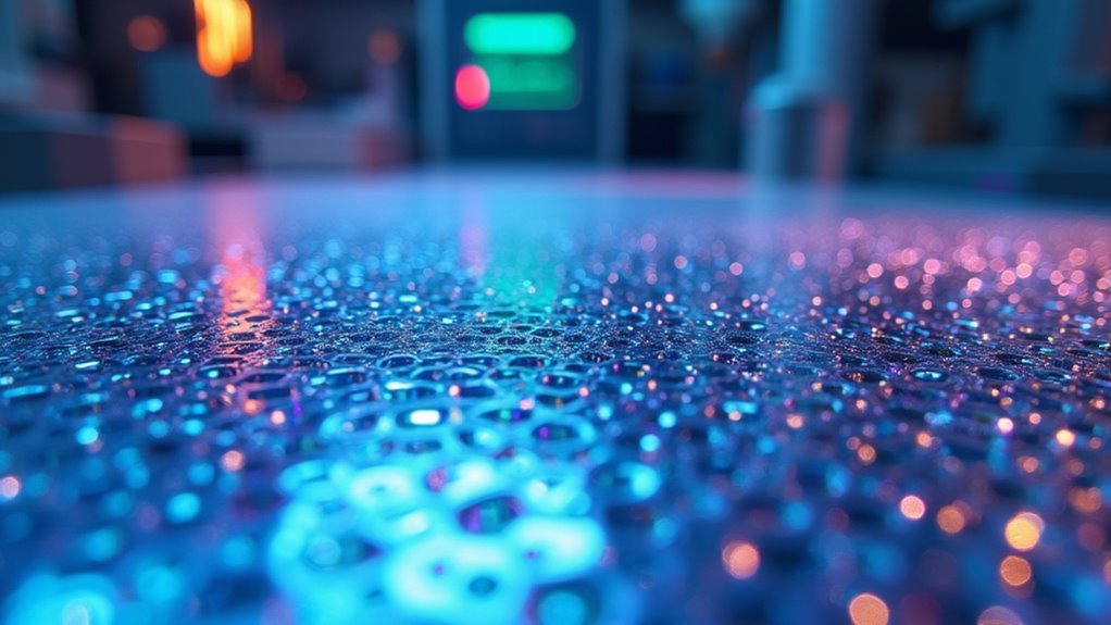
The Unique Properties of Graphene: A Foundation for 2D Materials
Graphene’s unique combination of properties establishes it as a foundational material for 2D materials.
You’ll notice it’s about 200 times stronger than steel yet five times lighter than aluminum, thanks to its hexagonal lattice of carbon atoms. Its atomic thickness of just 0.345 nm makes it incredibly flexible, allowing it to bend without breaking. Its high resistance also contributes to its durability in various applications, making it suitable for use in environments where strength and resilience are critical. Graphene also exhibits high elasticity, stretching and returning to shape repeatedly. Its outstanding electrical conductivity surpasses copper, while its thermal conductivity enables efficient heat dissipation. Additionally, the atomic thinness of graphene facilitates the development of flexible electronic devices and wearable technology. Despite being only one atom thick, it’s nearly transparent, absorbing just 2.3% of light. The vast surface area—around 2630 m²/g—opens doors for advanced sensors and transparent electronics. Plus, every atom is exposed, making it highly reactive and easy to functionalize for diverse applications.

Everything You Need to Ace Biology in One Big Fat Notebook
As an affiliate, we earn on qualifying purchases.
Exploring the Family of 2D Materials: Beyond Graphene
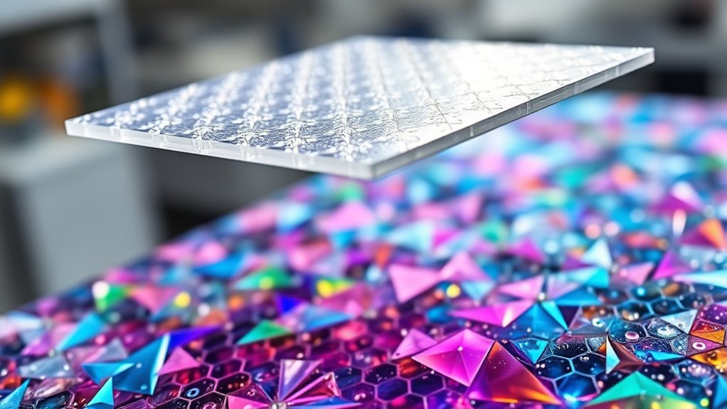
Building on graphene’s remarkable properties, researchers have identified a diverse family of 2D materials that expand the possibilities for electronics, energy, and sensing technologies.
Transition Metal Dichalcogenides (TMDs) like MoS₂ and WSe₂ are semiconductors with a direct bandgap at monolayer thickness, ideal for transistors and photodetectors. They also exhibit strong spin-orbit coupling and valley polarization, useful for spintronics.
| Material | Key Features |
|---|---|
| Hexagonal BN (hBN) | Wide bandgap (~5.9 eV), excellent dielectric properties |
| Black Phosphorus | Tunable bandgap (0.3-2 eV), high mobility |
| MXenes | Metallic conductivity, hydrophilic surfaces |
| Other 2D Materials | Diverse oxides, nitrides, sulfides, broad applications |
This family broadens the scope for innovative applications beyond graphene’s capabilities.

Earth Science: a QuickStudy Laminated Reference Guide (Quickstudy Reference Guide)
As an affiliate, we earn on qualifying purchases.
Techniques for Synthesis and Fabrication of 2D Layers

Techniques for synthesizing and fabricating 2D layers are essential for advancing research and practical applications. Mechanical exfoliation peels layers from bulk crystals, producing high-quality monolayers but with low yield and labor intensity.
Liquid-phase exfoliation disperses bulk materials in liquids using ultrasonication or shear forces, enabling larger-scale production but often results in smaller lateral sizes and defects.
MXenes, a prominent family of 2D materials, are created by chemically etching MAX phases, offering new functionalities.
Chemical vapor deposition (CVD) grows large-area, uniform monolayers by decomposing gaseous precursors on substrates, with in situ doping possible for tailored properties.
Physical vapor deposition (PVD) vaporizes solids onto substrates, providing controlled thickness.
These methods are crucial for exploring and producing diverse 2D materials beyond graphene, balancing quality, yield, and scalability.

The Elements Book: A Visual Periodic Table Encyclopedia for Kids (DK Our World in Pictures)
As an affiliate, we earn on qualifying purchases.
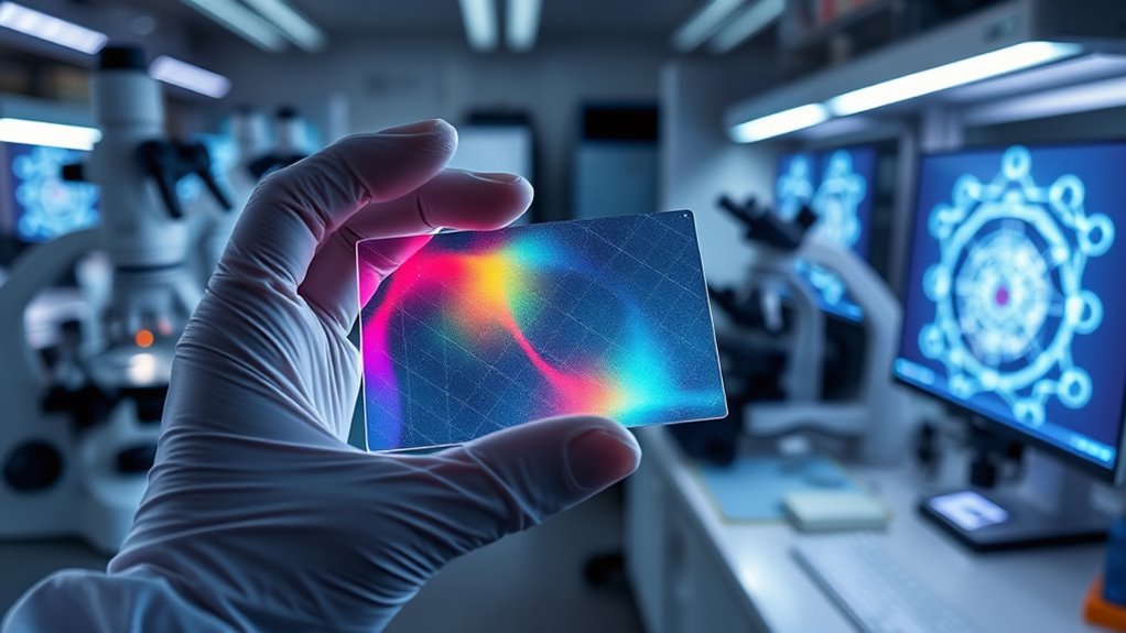
Innovations in Electronics and Photonics With 2D Materials

Innovations in electronics and photonics leveraging 2D materials are transforming how devices operate at both the fundamental and application levels. You benefit from ultra-high electron mobility in graphene (~200,000 cm²/Vs), enabling faster transistors and flexible circuits. Graphene’s exceptional electrical properties facilitate the development of high-speed, energy-efficient electronic components that outperform traditional materials. Semiconductor bandgap engineering through 2D heterostructures like MoS₂/WSe₂ allows for tunable logic devices. Hybrid integration with silicon supports advanced photodetectors, terahertz components, and sensors. The mechanical robustness and transparency of 2D materials make flexible electronics dominant, outperforming rigid silicon. Light manipulation is enhanced by broadband absorption, subwavelength confinement, and nonlinear optical effects useful in ultrafast lasers and modulators. Active plasmonics in graphene create tunable metasurfaces for dynamic light control, paving the way for scalable photonic circuits in telecom and LiDAR applications. Additionally, the unique electronic properties of 2D materials enable new paradigms in quantum and neuromorphic computing, opening avenues for next-generation information processing technologies.
Overcoming Challenges in 2D Materials Research and Development

Advancing the potential of 2D materials in electronics and photonics depends heavily on overcoming key research and development challenges. Synthesis hurdles include diverse chemistries, scalable methods, defect control, flake size, and cost issues. Environmental concerns involve nanoscale effects, biodegradability, ecological impact, regulations, and green synthesis. Property optimization requires postsynthetic modifications, accurate models, bridging experimental-theoretical gaps, and understanding quantum effects. Integration challenges focus on heterostructures, moiré systems, interfacial control, substrate compatibility, and device fabrication. Addressing these obstacles is essential for practical applications and sustainable development. Incorporating advanced sound design techniques can also aid in visualizing and communicating these complex scientific concepts more effectively.
Future Perspectives and Emerging Opportunities in 2D Material Technologies
The integration of 2D materials into semiconductor technologies is transforming the landscape of electronics, enabling devices that surpass traditional silicon limits. You’ll see atomically thin transistors, monolithic 3D integration, and hybrid silicon-2D systems pushing performance beyond current boundaries. These advancements are driven by the unique physical and chemical properties of 2D materials, which offer unprecedented opportunities for miniaturization and performance enhancement. Companies like TSMC, Intel, and IMEC are investing heavily in scaling up production, emphasizing new tooling for growth, characterization, and circuit design. Emerging applications include ultra-thin, flexible electronics, quantum devices, and advanced sensors with high surface area and conductivity. In energy, 2D materials boost batteries, supercapacitors, and renewable energy devices. The future also involves exploring novel 2D materials and heterostructures, broadening functionalities and creating multifunctional, customizable devices for electronics, energy, and quantum technologies.
Frequently Asked Questions
How Do Defects Affect the Electronic Properties of 2D Materials?
Defects markedly impact your 2D materials’ electronic properties. They can introduce new energy states, alter the bandgap, and change conductivity by acting as dopants or trap centers.
Vacancy and substitution defects modify how electrons move, affecting carrier mobility and device performance.
Grain boundaries and adatoms can increase scattering, reducing efficiency.
Can 2D Materials Be Integrated With Traditional Semiconductor Devices?
You might wonder if 2D materials can smoothly blend with traditional semiconductors. The answer is yes, but it’s a nuanced process.
You’ll find that integration requires careful techniques like van der Waals transfer or single-step stacking, which preserve material quality.
Challenges like interface compatibility and thermal limits exist, but ongoing research and collaboration are steadily paving the way for seamless hybrid devices that harness the best of both worlds.
What Environmental Factors Influence the Stability of 2D Materials?
You need to contemplate several environmental factors that impact the stability of 2D materials. Air exposure can cause hydrocarbon adsorption, changing surface and electrochemical properties.
Water contact affects wettability, while high temperatures above 250°C promote oxidation.
Humidity accelerates degradation, especially in less resistant materials.
Light exposure leads to photodegradation, and pollutants can cause chemical contamination.
Protecting these materials with coatings and controlled storage helps maintain their stability.
Are There Scalable Methods for Producing Defect-Free Large-Area 2D Layers?
Think of building a perfect mosaic; each piece must fit flawlessly. You ask if scalable methods exist for defect-free large-area 2D layers. Luckily, solution-based exfoliation techniques are advancing, enabling high-shear mixing and fluid dynamics control to produce large, high-quality sheets.
While challenges remain, especially for wafer-scale perfection, ongoing innovations focus on minimizing defects, maintaining integrity, and integrating processes for consistent, industrial-scale production.
How Does Stacking Order Impact the Electronic Behavior of Heterostructures?
You find that stacking order substantially impacts the electronic behavior of heterostructures. It controls interlayer interactions, which adjust band gaps, band splitting, and orbital hybridization.
By changing stacking configurations, you can tune spin polarization, electronic properties, and even induce unusual phenomena like massive electrons.
External factors like pressure further enhance these effects, giving you a powerful way to customize electronic characteristics for various applications.
Conclusion
While some might worry about the practical challenges of integrating 2D materials, their remarkable properties and ongoing innovations make them worth exploring. You’ll find that as research advances, scalable production and stability improve, opening doors to transformative applications. Don’t dismiss these materials as merely scientific curiosities—they’re poised to revolutionize electronics, energy, and beyond. Embrace the potential, because the future of 2D materials isn’t just promising; it’s within your reach.