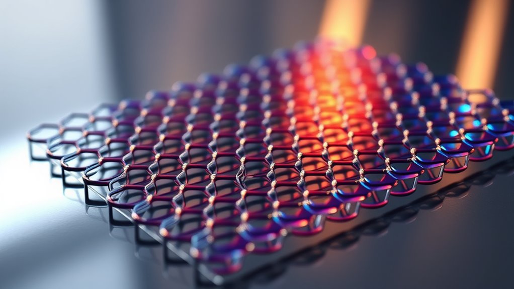

The 2D materials landscape, led by graphene, is expanding rapidly with innovative compounds and composites. You can harness heterostructure integration to create multifunctional, ultra-thin devices, while defect engineering helps optimize properties like conductivity and catalytic activity. Combining these strategies enables the development of high-performance, flexible, and energy-efficient technologies. Advances in scalable fabrication techniques ensure these materials can reach commercial applications. Keep exploring how these innovations are shaping the future of electronics, energy, and sensing devices.

Get school and study supplies delivered free — and shop member deals
- Fast, free delivery on millions of items
- Access to Prime Big Deal Days deals on October 6–7
- Prime Video, Amazon Music and more included
Key Takeaways
- The 2D materials landscape includes graphene, transition metal dichalcogenides, and other layered compounds with diverse electronic and optical properties.
- Heterostructure integration enables multifunctional devices by stacking different 2D materials for tailored performance.
- Defect engineering enhances conductivity, catalytic activity, and optical responses within 2D materials.
- Scalable fabrication techniques are advancing commercial applications of 2D heterostructures and defect-controlled systems.
- Future developments focus on innovative architectures and functionalities, revolutionizing electronics, sensing, and energy storage technologies.
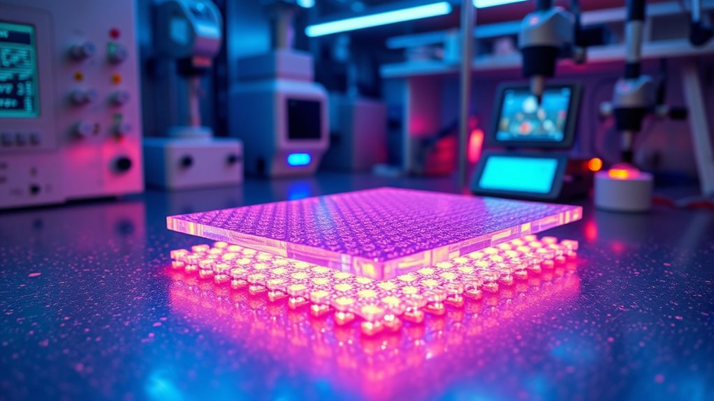
The 2D materials landscape is rapidly transforming the way we approach technology and science. You’re at the forefront of this revolution, where the ability to manipulate materials at an atomic scale unlocks unprecedented possibilities. One of the key advancements is heterostructure integration, which involves stacking different 2D materials to create complex, multifunctional systems. By carefully designing these layered structures, you can tailor electronic, optical, and mechanical properties to suit specific applications. This approach allows for the development of ultra-thin, flexible devices that outperform traditional materials. It also opens doors to innovative architectures in transistors, sensors, and energy storage, where the synergy between layers enhances performance beyond what individual materials could achieve.
Alongside heterostructure integration, defect engineering plays a pivotal role in optimizing 2D materials. You can deliberately introduce or control defects within the material’s lattice to modulate its properties. For example, creating vacancies or substitutional defects can enhance electrical conductivity, catalytic activity, or even influence optical responses. This precision defect manipulation enables you to fine-tune materials for specific functions, making them more efficient and versatile. It’s a powerful tool, especially when combined with heterostructure strategies, because it allows you to engineer interfaces and internal regions of layered systems for optimal performance. Whether you’re designing a next-generation transistor or a highly sensitive sensor, defect engineering helps to maximize the potential of each material.
The ability to integrate different 2D materials through heterostructure assembly, combined with defect engineering, means you’re no longer limited to the intrinsic properties of individual layers. Instead, you can craft bespoke systems with tailored functionalities. For instance, stacking graphene with transition metal dichalcogenides can produce heterostructures that exhibit unique electronic band alignments, enabling novel device concepts. Simultaneously, controlling defects within these layers can improve charge transfer, reduce noise, or boost catalytic activity. This synergy accelerates the development of high-performance, miniaturized devices that are flexible, lightweight, and energy-efficient.
You’re also witnessing the emergence of scalable fabrication techniques that make heterostructure integration and defect engineering more practical for commercial applications. As these methods become more refined, you’ll be able to produce complex 2D systems with high precision and reproducibility. This progress ensures that the benefits of these advanced materials—like enhanced conductivity, tunable optical properties, and mechanical resilience—are accessible at an industrial scale. Ultimately, the integration of heterostructure and defect engineering strategies is shaping a future where 2D materials are central to technological innovation, empowering you to design smarter, more efficient devices that were once thought impossible.
graphene flexible electronic devices
As an affiliate, we earn on qualifying purchases.
As an affiliate, we earn on qualifying purchases.
Frequently Asked Questions
What Are the Environmental Impacts of 2D Material Production?
You should know that producing 2D materials can impact the environment through a significant environmental footprint, mainly from energy-intensive processes and chemical use. Recycling challenges also exist, as recovering and reusing these materials isn’t straightforward, which can lead to waste. By understanding these impacts, you can support efforts to develop greener production methods and improve recycling techniques to minimize environmental harm.
How Scalable Are Manufacturing Techniques for Novel 2D Materials?
You’ll find that manufacturing techniques for novel 2D materials face scalability challenges, but ongoing manufacturing innovations are making progress. Techniques like chemical vapor deposition and exfoliation are being refined for larger-scale production, though maintaining quality and consistency remains a hurdle. As these innovations continue, you’ll see increased potential for commercial applications, making the production of 2D materials more scalable, cost-effective, and suitable for widespread use.
What Are the Potential Health Risks Associated With 2D Materials?
You should be aware that 2D materials pose potential health risks, including nanoparticle toxicity and inhalation hazards. Exposure during manufacturing or handling can lead to respiratory issues, skin irritation, and cellular damage. To protect yourself, always use proper safety equipment, work in well-ventilated areas, and follow safety guidelines. Staying informed about these risks helps you mitigate exposure and ensures safer use of these innovative materials.
How Do 2D Materials Compare Cost-Wise to Traditional Materials?
You’ll find that 2D materials often have higher initial costs compared to traditional materials, but their cost efficiency can improve over time due to enhanced performance and durability. Their unique properties may reduce the amount needed for certain applications, boosting market competitiveness. While upfront expenses might be higher, investing in 2D materials can lead to long-term savings and innovative product development, making them increasingly attractive in various industries.
What Are the Current Commercial Applications of Emerging 2D Materials?
You know what they say, “the future is now.” Emerging 2D materials find commercial use in flexible electronics, offering lightweight, bendable devices that last longer. They also revolutionize energy storage, with batteries and supercapacitors boasting improved capacity and charge times. These innovations are transforming industries, making devices more versatile and efficient. As these materials become more affordable, expect even broader applications across tech, healthcare, and renewable energy sectors.
Conclusion
As you explore the vibrant world of 2D materials, envision a future where graphene’s shimmering sheets reveal doors to endless possibilities. Picture a landscape painted with ultrathin layers, each one whispering promises of revolutionary tech. With every atom aligned, you’re on the brink of opening innovations that could reshape our world. Dive deeper, and let these tiny marvels inspire your imagination—because in this domain, the only limit is what you dare to envision.
Halloween Picks
halloween
As an affiliate, we earn on qualifying purchases.