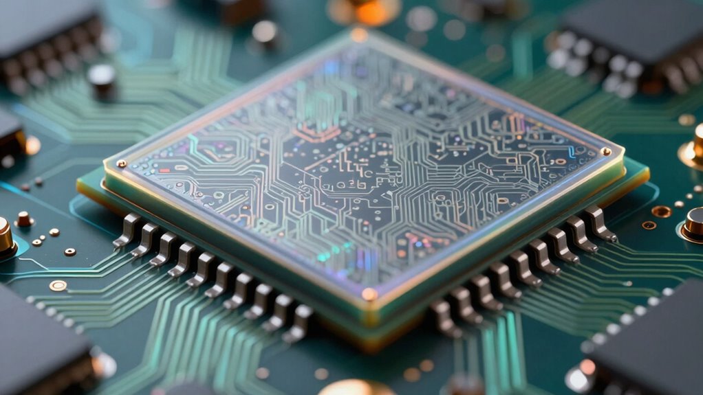

As electronics become more complex, you need better insulation chemistry to keep devices fast and energy-efficient. Low-k dielectrics reduce parasitic capacitance, improving device speed and lowering power consumption. Advanced deposition techniques guarantee these materials are reliable and defect-free, while eco-friendly innovations lessen environmental impact. If you keep exploring, you’ll discover how ongoing advancements in insulation chemistry support smarter, greener electronic devices and enhance overall performance.

Prime made for students and young adults
- Fast, free delivery for dorm and study essentials
- Prime Video and Amazon Music included
- Member-only deals
Key Takeaways
- Improved insulation chemistry reduces parasitic capacitance, increasing device speed and energy efficiency.
- Advanced dielectric materials enable smaller, more powerful, and reliable electronic components.
- Sustainable chemistry practices lessen environmental impact and support stricter industry regulations.
- Innovations in low-k materials balance high performance with eco-friendly manufacturing processes.
- Better insulation chemistry facilitates the development of faster, greener, and more compact electronic devices.
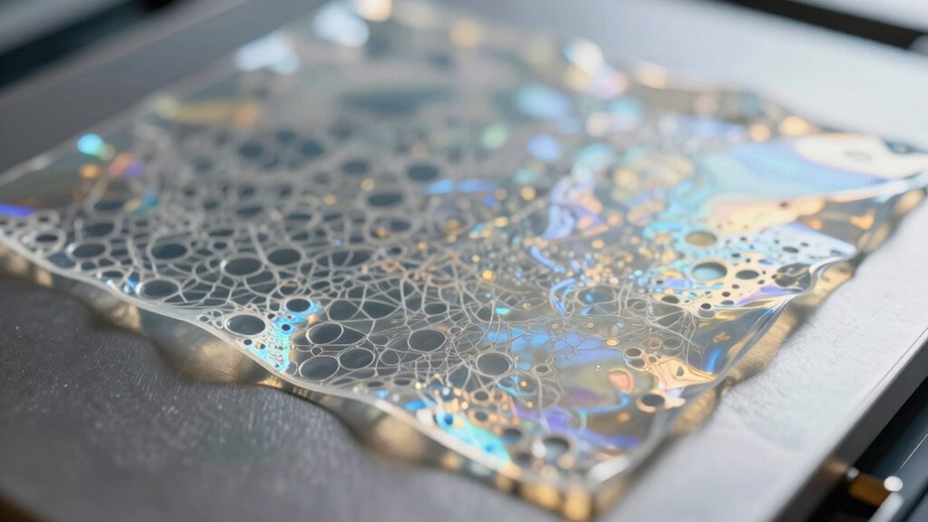
Have you ever wondered how modern electronic devices become faster and more efficient? The answer lies in the materials that insulate and protect the tiny components inside your gadgets. Low-k dielectrics are a fundamental part of this puzzle, helping to reduce parasitic capacitance in integrated circuits. As device architectures grow more complex, the need for materials with lower dielectric constants becomes essential. You might not think about it daily, but the chemistry behind these materials directly impacts your device’s speed, power consumption, and overall performance. That’s why researchers and engineers constantly explore new ways to improve low-k dielectrics, often turning to advanced deposition techniques to create ultra-thin, uniform layers. These techniques, such as chemical vapor deposition (CVD) and atomic layer deposition (ALD), allow for precise control over film thickness and composition, ensuring the dielectric layers are both effective and reliable. With these methods, you get a consistent, defect-free coating that minimizes leakage currents and enhances the device’s speed and efficiency. Additionally, ongoing research into advanced deposition techniques seeks to optimize the environmental impact of manufacturing processes, making them safer and more sustainable. However, as you push for better performance, environmental impact considerations must also come into play. Many traditional deposition processes involve hazardous chemicals and generate waste that can harm the environment. As a responsible engineer or consumer, you should be aware that the industry is shifting toward greener alternatives. Innovative approaches aim to reduce toxic emissions, lower energy consumption, and eliminate the use of harmful substances in manufacturing low-k dielectrics. This shift not only benefits the planet but also helps manufacturers comply with stricter regulations, leading to safer, more sustainable production methods. By adopting environmentally conscious deposition techniques, the industry creates materials that are both high-performing and eco-friendly, aligning technological advancement with environmental stewardship. Furthermore, the development of low-k dielectrics isn’t just about performance; it’s about balancing functionality with sustainability. The challenge lies in designing materials that meet the demanding electrical standards while minimizing environmental impact. This involves exploring new chemical formulations, such as porous materials that lower the dielectric constant without sacrificing stability. These innovations require careful research into how different deposition methods influence the final properties of the dielectric layer, including their environmental footprint. As you consider the future of electronics, it’s clear that progress depends on integrating advanced deposition techniques that prioritize both technological excellence and environmental responsibility. Ultimately, better insulation chemistry isn’t just about making devices faster or smaller—it’s about creating a smarter, greener future for electronics.
low-k dielectric materials for electronics
As an affiliate, we earn on qualifying purchases.
As an affiliate, we earn on qualifying purchases.
Frequently Asked Questions
How Do Low-K Dielectrics Impact Overall Device Performance?
Low-k dielectrics improve your device performance by reducing capacitance, which speeds up signal transmission and lowers power consumption. They also enhance material stability, preventing degradation over time. By having lower dielectric constants, these materials minimize crosstalk and electromagnetic interference, leading to more reliable operation. Overall, their use results in faster, more efficient electronics with longer lifespan, making your devices more durable and energy-efficient.
What Are the Environmental Concerns With Low-K Materials?
You should know that low-k materials raise environmental concerns because their production often involves hazardous chemicals, leading to environmental impact. These materials also pose sustainability challenges since they can be difficult to recycle or dispose of safely. As you develop or use electronics, consider how the environmental impact and sustainability challenges of low-k dielectrics influence eco-friendly design and responsible manufacturing practices, helping reduce harmful effects on the planet.
How Does Manufacturing Affect Low-K Dielectric Properties?
Think of manufacturing as the sculptor shaping fragile clay — it directly influences your low-k dielectric’s material stability and chemical composition. During production, exposure to high temperatures, chemicals, and etching processes can weaken the material, causing cracks or increased dielectric constant. These changes undermine insulation performance, making your electronics more vulnerable. Precision in manufacturing guarantees the dielectric maintains its properties, safeguarding your devices’ longevity and efficiency.
Are Low-K Dielectrics Compatible With Existing Semiconductor Processes?
You’ll find that low-k dielectrics are generally compatible with existing semiconductor processes, but material stability can be a concern. You need to carefully select materials that withstand processing conditions to prevent degradation. Cost considerations also come into play, as some low-k materials are expensive or complex to implement. By balancing stability and cost, you can integrate low-k dielectrics effectively, enhancing device performance without disrupting current manufacturing workflows.
What Are the Future Innovations in Low-K Dielectric Chemistry?
Future innovations in low-k dielectric chemistry focus on nanostructure optimization and enhancing chemical stability. You’ll see new materials engineered at the nanoscale to reduce dielectric constants further while maintaining mechanical strength. Researchers aim to develop more chemically stable compounds that resist moisture and thermal stress, ensuring reliable performance in advanced semiconductor devices. These advancements will enable faster, more efficient electronics, pushing the boundaries of miniaturization and insulating performance.
Conclusion
As you venture deeper into the world of electronics, think of low-k dielectrics as the silent guardians, weaving a delicate web of insulation that shields your devices from chaos. Their chemistry is like a finely tuned symphony, ensuring every component plays in harmony. Embrace the quest for better insulating materials, and you’ll be crafting a fortress of reliability, where each tiny molecule stands like a steadfast sentinel, safeguarding your technology’s future in a universe of shimmering connections.
Halloween Picks
halloween
As an affiliate, we earn on qualifying purchases.